TOKYO BOEKI participated in the International Exhibition SEMICON JAPAN 2019
Tokyo Boeki participated in International Exhibition the SEMICON JAPAN 2019 In partnership with Minimal Fab Promoting Organization which held in December 11-13, 2019 at the Exhibition Center Tokyo Big Sight at Tokyo. Here was possible to check and to get information about current line-up of Minimal Fab for microelectronic production such as current line-up of Minimal Fab for microelectronic production such as cleaning, coating and photoresist removal, photolithography, EB lithography, EB deposition, oxidation, PVD and CVD deposition, etching, diffusion and implantation, inspection, packaging.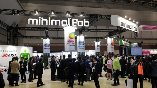
At exhibition were announced a new tools and improvements to Minimal Fab technology. In particular, a fully working and commercially available tool of Electron Beam Exposure was presented for electron beam direct exposure with improved characteristics, namely with a minimal line width 200 nm and an exposure speed of 5 min/mm2 at 10 kV and an irradiation dose of 30?C/cm2. Since the electron-optical column allows obtaining 2 nm resolutions, we expect to improve the minimal line width to 90 nm in the near future.
Also following working modules were presented at the exhibition such as TXRF Tester, Multi-Target Sputtering, Acetone-IPA Cleaner, Water Plasma Asher, Inverter, Multi-Chip Bonder.
Inspection tool TXRF Tester based on the method of Total Reflection X-ray Fluorescence and allows to determine the thickness of the deposited layers on the substrate with high speed. For example, average thickness of TiN with 30 nm can be measured in 30 seconds. The TXRF Tester module allows multi-point measurement by mapping and is equipped with a function to measure metal contamination on the wafers.
Multi-Target Sputtering tool is a system for three target metal deposition. Deposition source is based on a frequency-tuning compact helicon plasma source is attached on the side wall of the compact vacuum chamber and the plasma is transported along curved magnetic field lines to a target surface, which is mounted on a rotational target holder and negatively biased by a dc power supply. The target material is sputtered by the ions accelerated by the sheath potential drop and deposited on the substrate facing the target. The target material can be changed by rotating the holder; thereby the multi-layered metallic film can be formed in the single chamber. Substrate heating induced by secondary electrons emitted from the target surface and accelerated by the sheath is successfully inhibited by a magnetic filter near the substrate.
Acetone-IPA Cleaner is tool of cleaning for wafers with acetone and isopropyl alcohol.
Water Plasma Asher is toll for plasma etching and removal of photoresist. A new and unique method of resist removal (ashing with water plasma), which does not contain chemicals and have a small impact on the environment. This method generates a plasma with a low gas temperature in water vapor of ultrapure water, gasified by microwave radiation, and produces ashing using highly active components (OH radicals, etc.). Currently the high-speed resist removal has been achieved (>1 ?m/min) at the same time it provides high cooling effect due to direct contact of wafer with water.
Inverter tool for inverting wafers at cleanliness level conditions as in clean rooms.
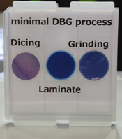
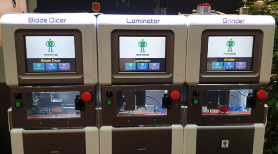
Addition to new products, DISCO Co. introduced the Dicing Before Grinding demo system, namely, the Grinder, Blade Dicer, Laminator tools with the ability to test these processes at the exhibition booth.
DISCO Co. also developed the new Minimal Shuttle robotic transfer system to ensure an automated process of medium series production.