Minimal Technology
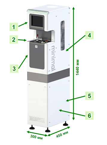 Compact semiconductor line-up have a one standardized chassis in Minimal format with size 300mm x 450mm × 1440mm (WxDxH), robotic loading system for wafer, control system and connection method for all devices:
(1) Control interface and PC.
(2) Loading place for Minimal Shuttle.
(3) PLAD system for wafer transfer from Minimal Shuttle to process chamber into the tool side.
(4) Process chamber and storage unit of consumables.
(5) External connection unit.
(6) Storage unit for used consumables.
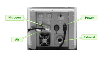
Unified external connection unit: for all Minimal tools:
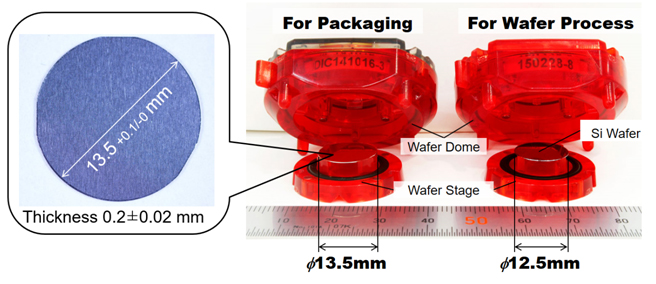
 A robotic and unified transport system PLAD (Particle Lock Air-tight Docking) was developed for the substrate transferring to all Minimal tools.
Depending on type of equipment and technology process there are two docking systems: atmospheric type and high-vacuum type.
Thus the wafer is always protected by a clean environmental (in a container) during upload from one process tool to another.
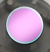
The transparent red material of Minimal Shuttle makes the wafer visible and blocks the ultraviolet radiation.
One type of container is used for all technological processes. In case of packaging the Minimal Shuttle differs only in diameter of wafer stage.
 |
List of available substrates for Minimal Fab technology: Si, Silicon on insulator (SOI), GaAs, GaN, Ga2O3, сапфир, алмаз, кварц, боросиликатное стекло. |
 |
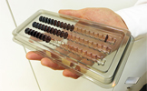
Shipping case for 40 wafers. |
 |
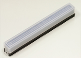
Wafer tray for 60 wafers. |
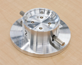 |
Manual opener for Minimal Shuttle. |
 |
Wafer cleaning holder on 40 wafers. |